
On April 29, 2025, Keysight and Intel Foundry announced a chip development partnership. These chips are mainly used in artificial intelligence and big data centers for cloud computing, online storage, and smart apps. Their collaboration will make it easier for individual components in a chip to communicate within the same package.
They are focused on a new technology called Embedded Multi-die Interconnect Bridge-T (EMIB-T). This special chip design method allows for the chip facilities to be divided into parts known as chiplets making them easier and faster to connect. With EMIB-T, the organizations can design the chips that will be better, quicker, more intelligent, and more efficient for the next generation of artificial intelligence and data structures.
Introducing EMIB-T: A Leap in Chip Packaging
EMIB-T is a shortened form of Embedded Multi-die Interconnect Bridge-T, a next-gen tech that connects many chiplets in one package. This innovation applies to the situation, as it handles complex AI and data center workloads by allowing high-speed data transfer and efficient power delivery between chiplets and 3D integrated circuits (3DICs).
This results in the fact that integrating EMIB-T can improve the performance and flexibility of chiplet-based architecture to meet SoC performance needs. This permits the incorporation of multiple functional blocks or chiplets in a product with specific functions, enhancing efficiency and possibly cutting costs and speeding up development
Embracing Open Standards: UCIe™ 2.0 and BoW
The collaboration promotes new interfacing standards such as the Universal Chiplet Interconnect Express™ (UCIe™) 2.0 and Bunch of Wires (BoW) from the Open Compute Project. These standards ensure chiplets can connect with components from other companies and suppliers, which would lead to creating a more expandable and versatile design in the industry.
Both of these open standards offer design freedom and greater AI and data center development potential. It also promotes a scaling chiplet interconnectivity market by cutting development costs and reducing proprietary risks
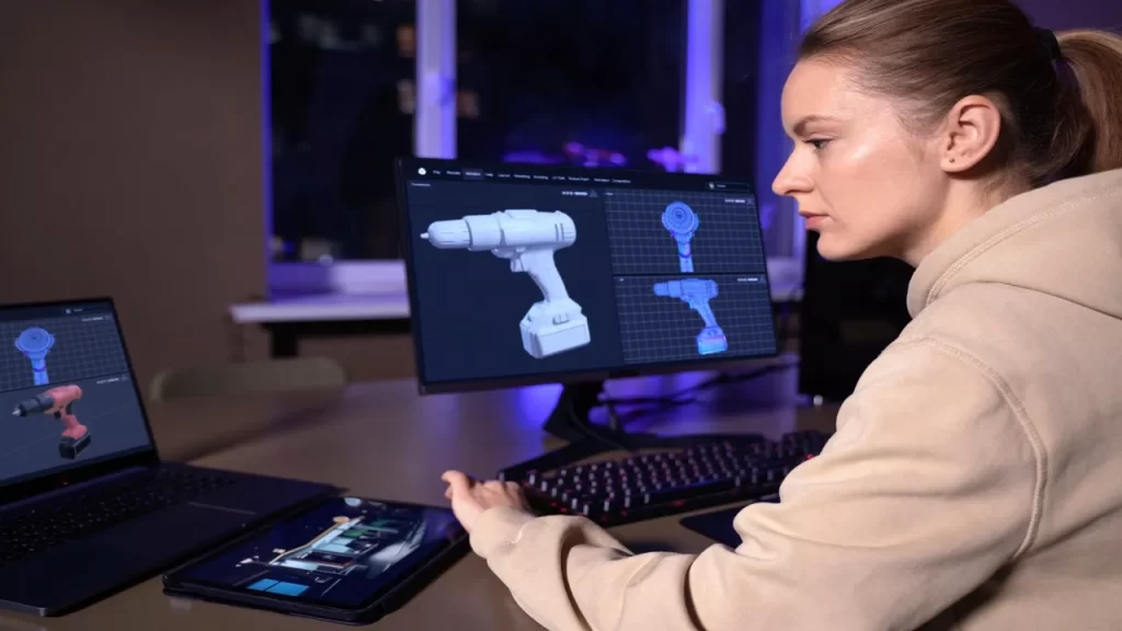
Keysight’s Chiplet PHY Designer: Streamlining Pre-Silicon Validation
Keysight’s EDA team has been working to improve Chiplet PHY Designer, and the latest version is EMIB-T compatible. It also supports the simulation of UCIe™ 2.0 and BoW standards to let engineers test chiplet designs before silicon.
It has been designed to make systems through chiplet creation and D2D integration easily achievable. It reduces costly redesigns and increases the overall pace at which new semiconductor applications are generated.
Demonstrating Innovation at Intel Foundry Direct Connect
The EMIB-T live demonstration was conducted by Keysight during the Intel Foundry Direct Connect event on 29th April at San Jose. This demonstration focused on showcasing the link performance and compliance capabilities at the system level of EMIB-T technology, which has applications in AI and data center operations.
This way, it becomes a perfect ground for the professional to discover new packaging technologies and form partnerships that would enable new semiconductor designs. Keysight’s presence was in line with its goal of supporting innovation in the field of chiplet interconnection.
Industry Leaders on Collaboration
According to today’s leading article, cited from Suk Lee, the vice president and general manager of Intel’s ecosystem technology office, a new cooperative agreement with Keysight EDA on the development of the Silicon bridge technology of EMIB-T, as compared to other techniques, is a novel advance in high form packaging. Thus, by adopting standards like UCIe™ 2.0, we increase the freedom of chiplet design for AI and data center clients and advance our clients’ ability to adjust to next-generation technology needs.
Niels Faché, Vice President and General Manager of Keysight’s Design Engineering Software, said, “Chiplet PHY Designer from Keysight EDA has once again revolutionized pre-silicon validation, providing the designers with the speed and accuracy in verifying chiplet architecture. With involvement involving new standards like the UCIe™ 2.0 and Bunch of Wires (BoW), Intel Foundry’s EMIB-T (Embedded Multi-die Interconnect Bridge-T), we are preparing to offer innovative engineers tactical ways of slashing design costs and iterations before manufacture.